Tokyo – May 28, 2025 – TOPPAN Inc. (TOPPAN), a TOPPAN Group company and wholly owned subsidiary of TOPPAN Holdings Inc. (TYO: 7911), will participate in JPCA Show 2025, which will be held at the Tokyo Big Sight international exhibition center from June 4 to 6.
JPCA Show enjoys a high profile both in Japan and overseas. It showcases the latest content and solutions, including electronic circuits, mounting technologies, sensors, and wearable technologies and aims to provide technical insights and new ideas to contribute to the growth of the electronic circuit sector and related industries.
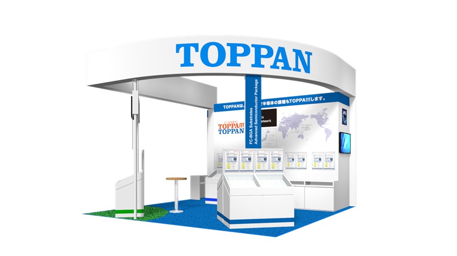
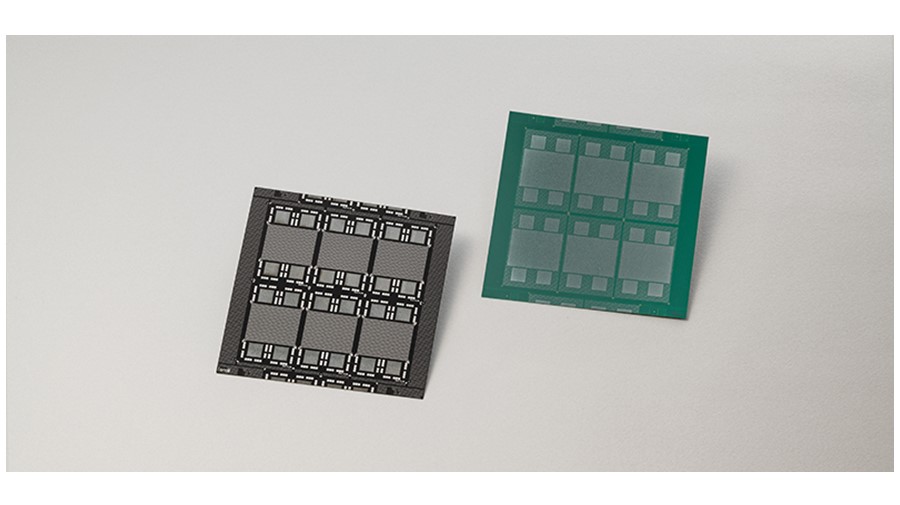
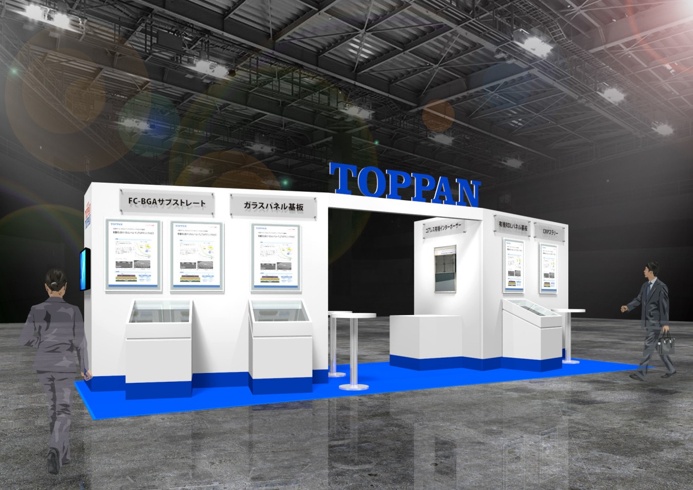
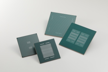
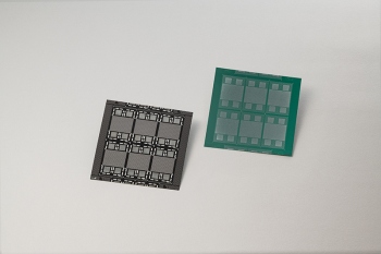
The TOPPAN booth at JPCA Show 2025 will present FC-BGA substrates as well as technologies and components for next-generation semiconductor packaging.
Main Solutions on Show
1) FC-BGA substrates
2) Next-generation semiconductor packaging
About JPCA Show 2025
・Dates & times: June 4 to 6, 2025 10:00—17:00
・Venue: Tokyo Big Sight, East Hall 7
*TOPPAN will participate in JPCA Show 2025 (East Hall 7/booth 7D-02)
・Organizer: Japan Electronics Packaging and Circuits Association
・Official website: https://www.jpcashow.com/show2025/en/index.html
2. A technology for creating spaces for mounting components on a substrate.
3. A substrate used for electrically connecting front and rear circuits with through-mold vias.
About the TOPPAN Group
Established in Tokyo in 1900, the TOPPAN Group is a leading and diversified global provider committed to delivering sustainable, integrated solutions in fields including printing, communications, security, packaging, décor materials, electronics, and digital transformation. The TOPPAN Group’s global team of more than 50,000 employees offers optimal solutions enabled by industry-leading expertise and technologies to address the diverse challenges of every business sector and society and contribute to the achievement of shared sustainability goals.
https://www.holdings.toppan.com/en/
https://www.linkedin.com/company/toppan/