Jan 14, 2014
Toppan Printing to install new manufacturing line for FC-BGA substrates
Expanded production capacity for leading-edge products for high-end LSI used in communication, gaming machines, and in-vehicle devices
Expanded production capacity for leading-edge products for high-end LSI used in communication, gaming machines, and in-vehicle devices
Toppan Printing Co., Ltd. (hereafter “Toppan Printing”; head office: Chiyoda Ward, Tokyo; President & Representative Director: Shingo Kaneko) will install new production equipment at its Niigata Plant (Shibata City, Niigata Prefecture) to expand FC-BGA (Flip Chip Ball Grid Array) substrate business in response to increasing demand brought about by the miniaturization and enhanced performance of LSI. The new line will be equipped with machinery capable of producing leading-edge products and be launched at the end of 2014. The total investment will be approximately ¥10 billion. This new line will increase Toppan Printing’s FC-BGA substrate production capacity to approximately 2.5 times its current level.
Background
Demand for FC-BGA substrates is expected to continue to grow as further miniaturization of LSI progresses. Even faster communication, lower power consumption, and higher density wiring are required in FC-BGA substrates for high-end LSI. In order to respond to these market needs, Toppan Printing will introduce a new line capable of manufacturing leading-edge substrates that are thinner, coreless, and have higher density wiring.
Demand for FC-BGA substrates is expected to continue to grow as further miniaturization of LSI progresses. Even faster communication, lower power consumption, and higher density wiring are required in FC-BGA substrates for high-end LSI. In order to respond to these market needs, Toppan Printing will introduce a new line capable of manufacturing leading-edge substrates that are thinner, coreless, and have higher density wiring.
Features
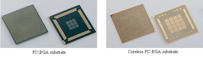
-Thinner substrates due to the use of thin core materials
The thickness of the FC-BGA substrate is reduced from 0.8 mm to 0.2 mm due to the core material, meaning LSI can be further downsized and transmission characteristics are improved.
-High-efficiency production line capable of manufacturing coreless FC-BGA substrates
As leading-edge coreless FC-BGA substrates do not use any core material, further miniaturization, higher density, weight reduction, and high-speed transmission can be achieved. To respond to increasing demand in the future, the new line will have significantly enhanced efficiency for the production of coreless FC-BGA substrates.
-Narrow pitch wiring
Existing FC-BGA substrates have a line/space of 15 µm (1 micrometer=1/1000 millimeter). However, in line with the miniaturization of LSI, the new line will be capable of producing line/spaces of 10 µm or less, making it possible to form fine wiring structures for LSI.
Future targets
Toppan Printing is aiming to achieve ¥20 billion in sales as early as possible.