© TOPPAN INC.
Tokyo – October 7, 2021 – Toppan (TYO: 7911), a global leader in communication, security, packaging, décor materials, and electronics solutions, has developed technology to manufacture glass microfluidic chips by photolithography.1 Mass production of microfluidic chips using the technology will make it possible to produce chips in larger volumes and at lower cost than those manufactured via current injection molding technology, which involves injecting polydimethylsiloxane (PDMS), a type of silicone resin, into a metal mold.
Photolithography is a fundamental technology honed by Toppan over 60 years in the electronics business and is used for microfabrication of LCDs and master plates for semiconductor circuits. Microfluidic chips manufactured by this technology are expected to be used in the fields of in-vitro diagnostics and liquid biopsy (a largely non-invasive diagnostic technology requiring only a small amount of blood or other fluid sample), which is expected to see high levels of demand for applications including cancer diagnosis and clinical testing.
Recent years have seen growing interest in liquid biopsy testing, which uses samples of blood or other fluids to enable super-early detection of cancer. Microfluidic chips manufactured by injection molding using PDMS are widely used for testing due to the material’s excellent biocompatibility and suitability for optical analysis. The low productivity for microfabrication when using PDMS and the high cost of liquid silicone as a raw material, however, drive up the cost of chips, presenting an obstacle to more widespread use.
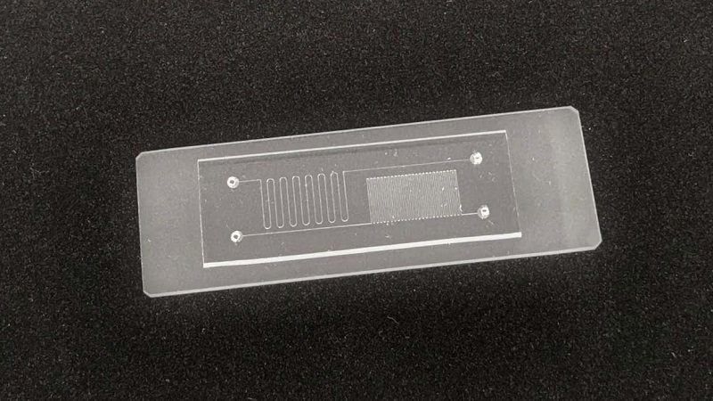
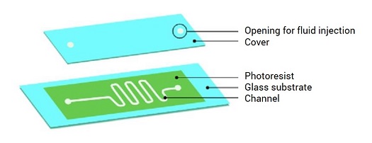
To address this challenge, Toppan has developed technology for producing microfluidic chips by applying microfabrication technology based on photolithography techniques cultivated in the manufacture of LCD color filters. Specifically, channels (grooves or holes that allow liquid or gas to flow) with a width of 10 micrometers (micrometer=0.001 millimeter) to several millimeters and a depth of one to 50 micrometers are formed on photoresist (light-sensitive material) coated onto a glass substrate. A cover with openings for injecting fluid samples or specimens is then applied over the cured photoresist. Microfluidic chips manufactured using this method have properties that are equivalent or superior to those of PDMS chips and can enable production in larger volumes and at lower cost.
© TOPPAN INC.
“We have applied Toppan’s advanced microfabrication techniques to potentially enable mass production of something that can drive widespread use of medical testing techniques that reduce the burden on patients,” said Yuichiro Abe, manager of Development Planning in Toppan’s Electronics Division. “We will continue to work with our collaborative partners on pilot testing for commercialization of glass microfluidic chips and hope to establish photolithography-based mass production technology by March 2022.”
Toppan’s new technology will be showcased in the Toppan booth (C-12, Exhibition Hall) at JACLaS EXPO 2021, an event focusing on clinical laboratory testing equipment, reagents, and systems, at the Pacifico Yokohama convention center from October 8 to 10.
Features of Toppan’s Microfluidic Chips
© TOPPAN INC.
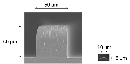
Microfluidic devices used for the analysis of blood, bacteria, and cells sometimes require deep channels with a depth of approximately 50 micrometers. By reassessing photoresist composition and the exposure process, Toppan has made it possible to provide optimal channel design for a wide range of analysis applications.
© TOPPAN INC.
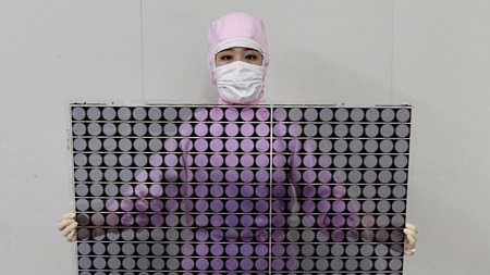
Production via multi-imposition of microfluidic chips on large glass substrates can be made possible by taking advantage of manufacturing equipment for LCD color filters used in digital devices such as smartphones, tablets, and PCs.
About JACLaS EXPO 2021
Dates: October 8 to 10, 2021
Times: 9:00‒17:30 (Ends at 14:00 on the final day)
Venue: Pacifico Yokohama, Exhibition Hall
Organizer: Japanese Association of Clinical Laboratory Systems (JACLaS)
https://jaclas.or.jp/en/
About Toppan
Established in Tokyo in 1900, Toppan is a leading and diversified global provider committed to delivering sustainable, integrated solutions in fields including printing, communications, security, packaging, décor materials, electronics, and digital transformation. Toppan’s global team of more than 50,000 employees offers optimal solutions enabled by industry-leading expertise and technologies to address the diverse challenges of every business sector and society and contribute to the achievement of shared sustainability goals.
For more information, visit https://www.toppan.com/en/ or follow Toppan on LinkedIn https://www.linkedin.com/company/toppan/.