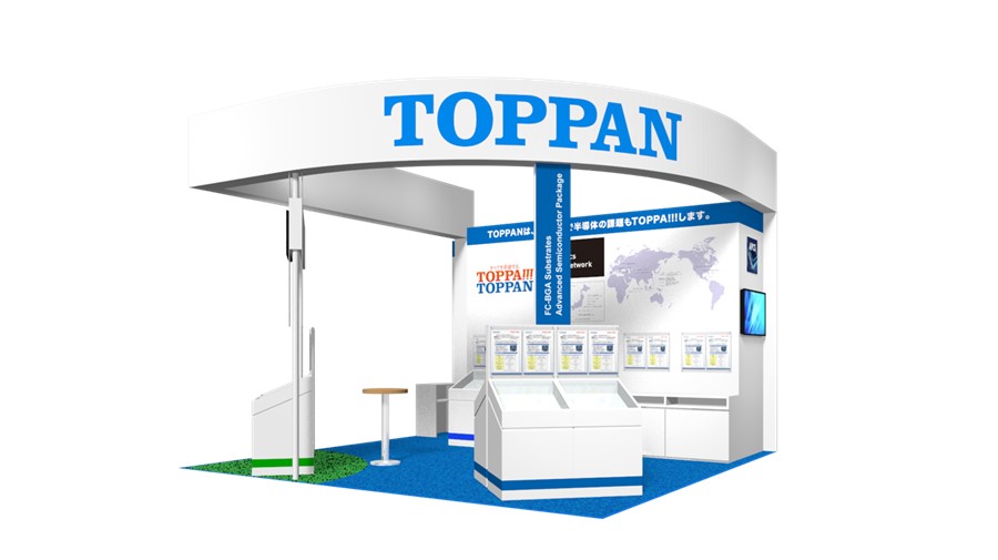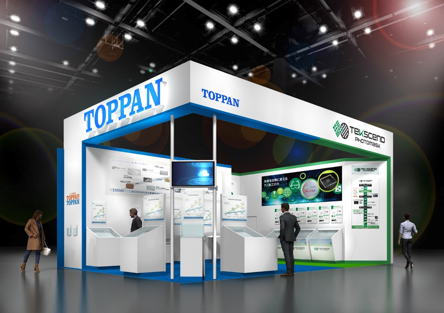
Tokyo – December 10, 2025 – TOPPAN Inc. (TOPPAN), a TOPPAN Group company and wholly owned subsidiary of TOPPAN Holdings Inc. (TYO: 7911), and Tekscend Photomask Corp. (TYO: 429A) (Tekscend Photomask) will join forces at SEMICON Japan 2025, which will be held from December 17 through 19 at the Tokyo Big Sight exhibition center.
SEMICON Japan is an international event focused on the electronics manufacturing sector. It covers semiconductor industry manufacturing technologies, equipment, and materials, as well as smart applications such as automobiles and IoT devices.
Positioning the semiconductor-related business as an area for proactive expansion, TOPPAN is working to expand production capacity for Flip Chip-Ball Grid Array (FC-BGA) substrates and develop advanced semiconductor packaging technologies. Anticipating an increase in demand related to AI and data centers, TOPPAN’s electronics business is targeting sustainable growth centered on semiconductor packaging.
Tekscend Photomask, a leader in the merchant market for semiconductor photomasks, is strengthening its development and production capabilities for technologies at advanced nodes. The company is expanding its global supply system while enhancing support for extreme ultra-violet (EUV) and other next-generation processes.
Main Solutions on Show
1) TOPPAN
・FC-BGA substrates
・Advanced semiconductor packaging
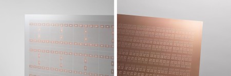
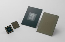
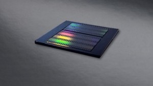
The TOPPAN Group booth at this year’s SEMICON Japan will showcase for the first time glass core FC-BGAs, which feature interconnects fabricated with a glass panel substrate as the core material. The booth will also feature organic redistribution layer (RDL) interposers that use glass carriers as well as glass panel substrates combining through-glass vias and cavities with different depths on the same glass.
・LSI design/turnkey services
As a provider of LSI development and design services for approximately 50 years, TOPPAN will present LSI design and turnkey services, ranging from leading-edge to mature processes, supporting a wide range of interfaces to meet customer requirements.
2) Tekscend Photomask
・EUV photomasks
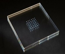
・Nanoimprint molds
Silicon nanoimprint molds
・Quartz nanoimprint molds
・Nanoimprint prototype development support
About SEMICON Japan 2025
Dates: December 17 to 19, 2025 10:00—17:00
Venue: Tokyo Big Sight
Organizer: SEMI
Official website: https://www.semiconjapan.org/en
TOPPAN Group booth: E6144 (East Hall 6)
About the TOPPAN Group
Established in Tokyo in 1900, the TOPPAN Group is a leading and diversified global provider committed to delivering sustainable, integrated solutions in fields including printing, communications, security, packaging, décor materials, electronics, and digital transformation. The TOPPAN Group’s global team of more than 50,000 employees offers optimal solutions enabled by industry-leading expertise and technologies to address the diverse challenges of every business sector and society and contribute to the achievement of shared sustainability goals.
https://www.holdings.toppan.com/en/
https://www.linkedin.com/company/toppan/
About Tekscend Photomask Corp.
Tekscend Photomask Corp. is the world's premier provider of photomasks for semiconductors. Headquartered in Tokyo, Tekscend leverages its worldwide customer service network and nine manufacturing facilities in key geographic locations to offer the world's most advanced photomask technology. Tekscend has also expanded into nanoimprint molds, waveguides and other nano-fabricated products. For more information, visit https://www.photomask.com/en.